
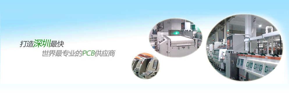
PCB (Printed circuit board, PCB) will appear in almost every electronic device which. If a sample
Equipment with electronic components, they are also set in different sizes on the PCB. In addition to a variety of small parts is fixed, PCB
The main function is to provide the top part of each electrical connection. As electronic devices increasingly complex, requiring more and more parts, PCB top of the line and the parts are increasingly dense. Standard PCB looks like this. Bare board (on top no parts) is often called the "PCB Printed Wiring Board (PWB)." Not easy to bend the material made . Can be seen on the surface material is a copper fine line, the original copper foil covering the whole board, and in the manufacturing process was partially etched away, leaving to become part of a network of fine lines . These lines are referred to as wire (conductor pattern) or said wiring, and to provide a circuit-connecting parts on the PCB. Parts to be fixed on the PCB
Above, we will take their feet welded directly on the wiring. At the most basic PCB (single panel), the parts are concentrated in the one side of the wire are concentrated on the other side. This way we need holes on the board, so that the pin can pass through the board to the other side, so the parts are welded pin on the other surface. Because of this, PCB are called positive and negative parts surface (Component Side) and the welding surface (Solder Side). There are certain parts such as PCB top, you need to be removed after production is completed or put back, then that part will be used when installing socket (Socket). Since sockets are soldered directly to the board, the parts can be any disassembly. Below you see the ZIF (Zero ion Force, Zero ion Force dial-in) jack, which allows parts (here refers to the CPU) can be easily ed the socket, it can be removed. Socket next to the lever, you can in your parts will be fixed if you want two PCB interconnected, generally we will use known as "Goldfinger" edge connector edge connector). Goldfinger contains many bare copper pads, these copper pad is in fact a part of PCB routing. Usually connected, we will be one of a finger on the PCB ed another piece of the appropriate slot on the PCB (commonly called expansion slots Slot). In a computer, such as graphics cards, sound cards, or other similar interface cards, are connected through the finger to the motherboard. Green or brown on the PCB, the solder mask (solder mask) color. This layer is an insulating protective layer can protect the wire, it can not prevent the parts are welded to the right place. The solder resist layer will be printed on the other side a layer of screen printing (silk screen). Usually in it will be printed on the text and symbols (mostly white), to mark out the parts on the board position. Also known silkscreen icon plane (legend). Single panel (Single-Sided Boards) we have just mentioned, at the most basic
PC, part concentrated on one side of the wire is concentrated on the other side. Because only in one side of the wire, so we call this PC is called a single panel Single-sided. Because the design circuit board there are many strict restrictions (since only one side of the wiring which must not cross a path around alone), the circuits so that only the early use of such a board. Two panels (Double-Sided Boards) on both sides of this wiring board. However, to use the wire on both sides, both sides must have the proper electrical connection between the job. This circuit between the "bridge" is called the pilot hole (via). Vias on the PCB is filled or coated with metal holes,